The Noise Measured by Back-illuminated Silicon Sensors
Roy T. Smart1, Charles C. Kankelborg1, and Jacob D. Parker2
1Montana State University
2NASA/GSFC
246th Meeting of the American Astronomical Society
June 9th, 2025


IRIS Noise Mystery
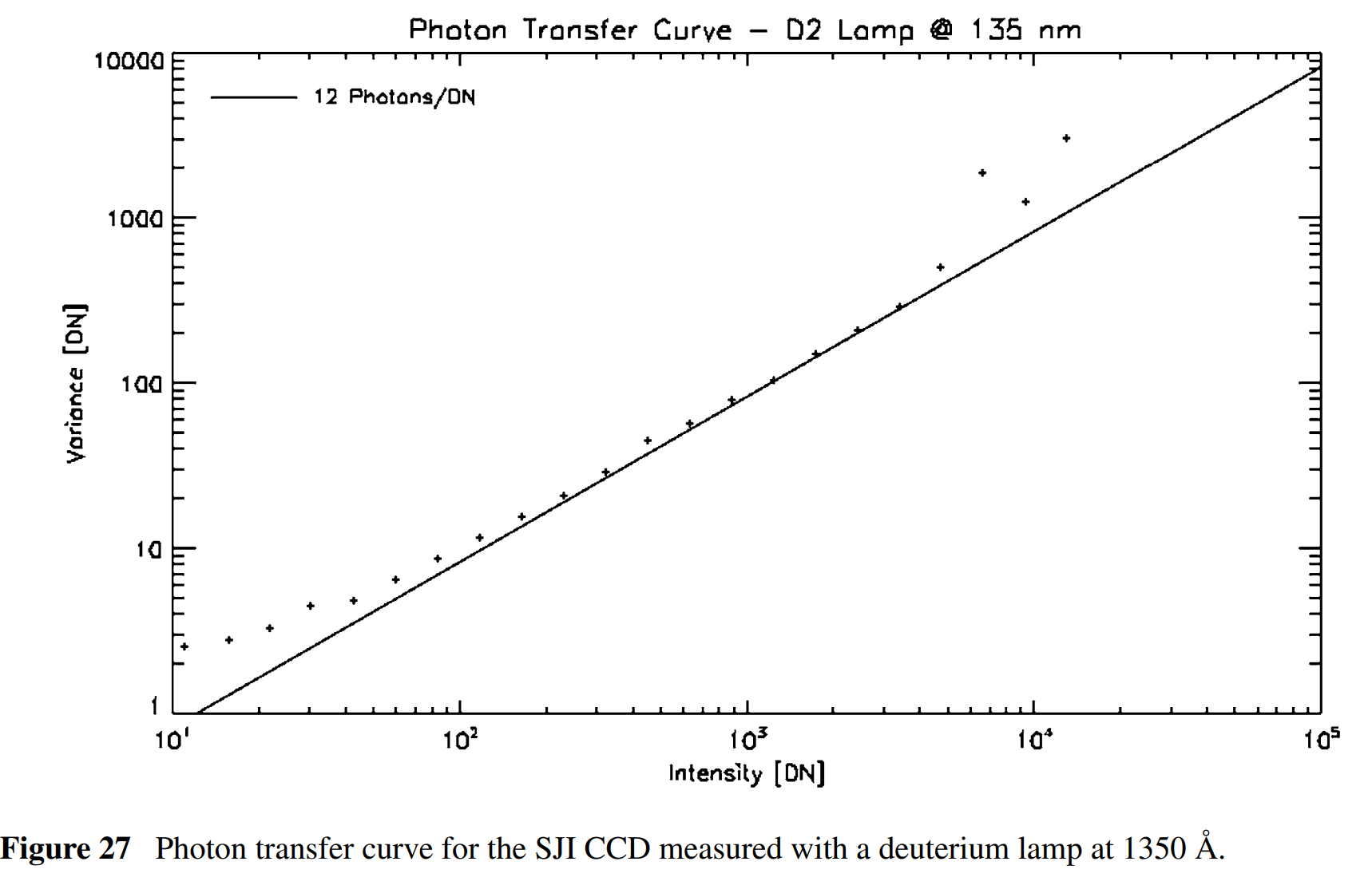
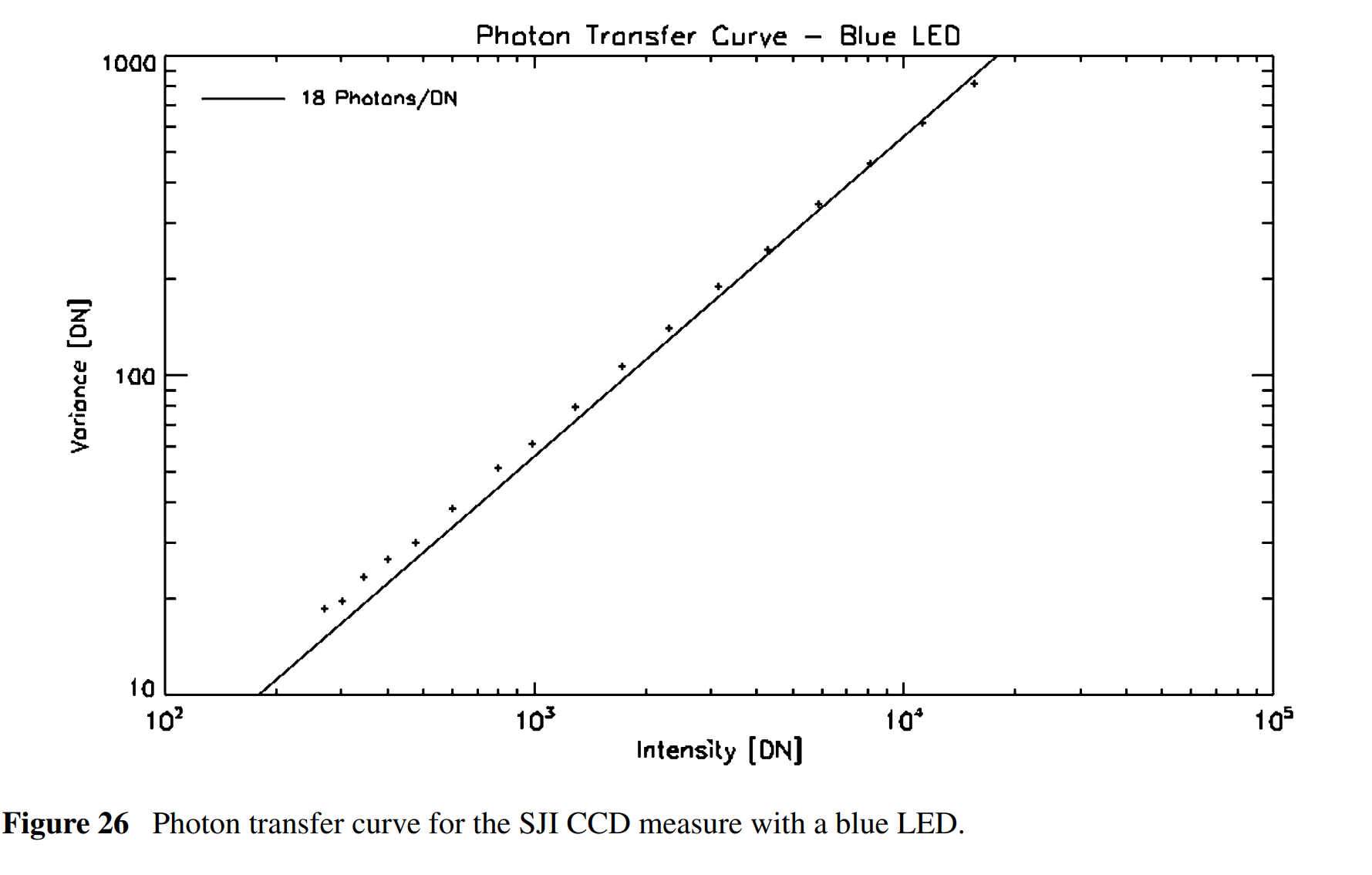
IRIS measures less noise than predicted (Wulser et al. 2018).
Photon transfer curve is too shallow
Expected slope ratio > 2
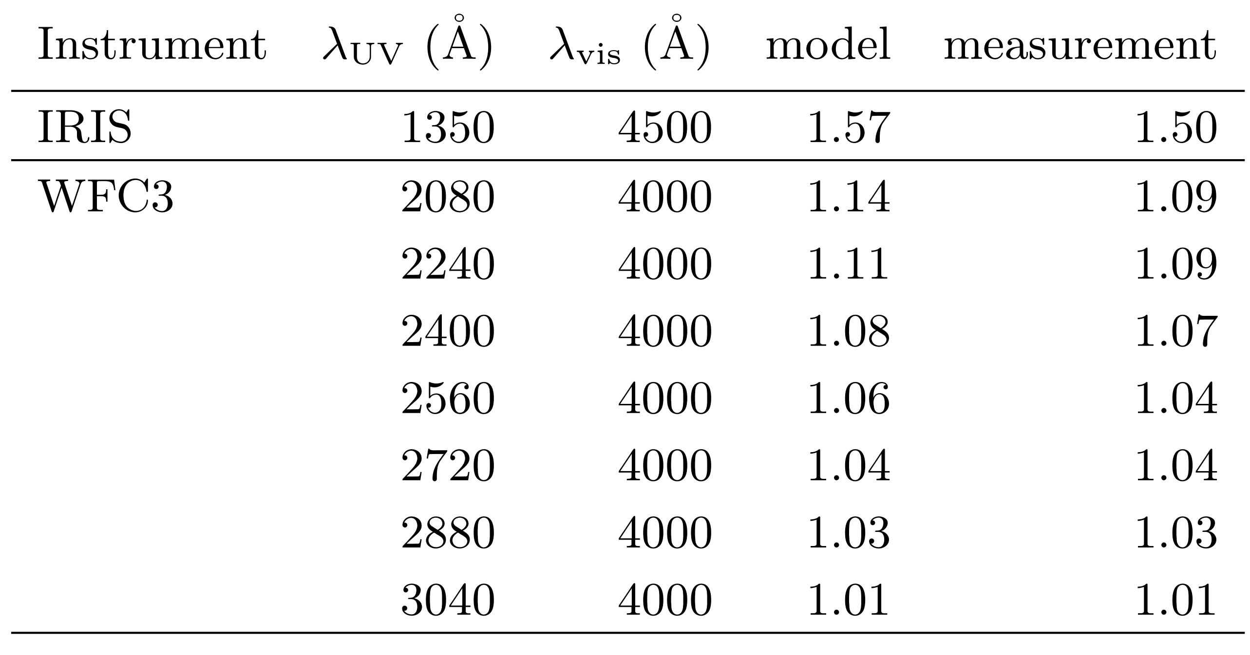
Measured slope ratio = 1.5
SNR is ~25% better than expected
HST/WFC3 Noise
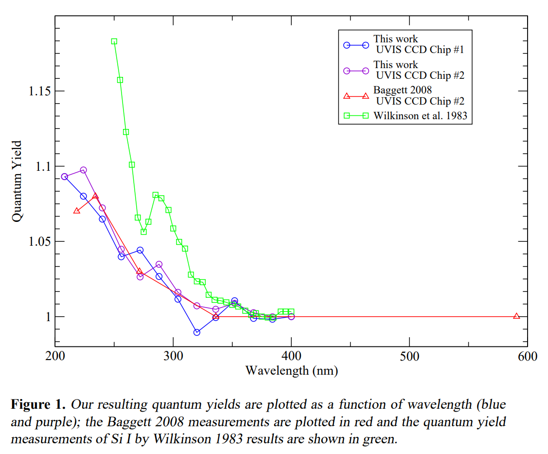
Wide Field Camera 3 (WFC3) on Hubble also has this issue (Marinelli & Green 2024)
“Quantum yield” is lower
Expected ~1.7 @ 200 nm
Measured 1.09 @ 200 nm
SNR is ~25% better than expected
Quantum Yield
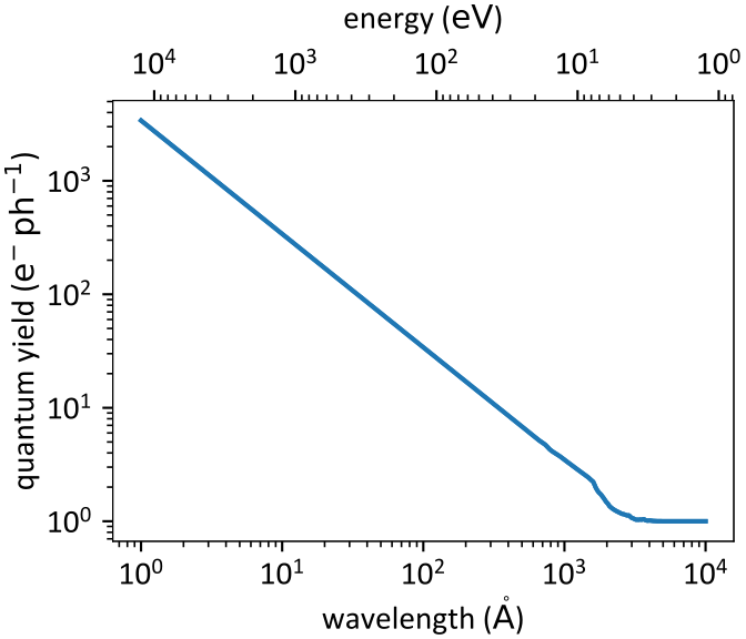
Quantum yield (QY) is the number of electron-hole pairs generated per photon
QY increases as photon energy increases
QY = E / (3.65 eV) where E is the energy of the photon
Ramanathan & Kurinsky (2020) QY model
Back-illuminated Sensor Model
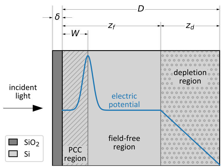
Thin layer of silicon dioxide (~1 nm)
Light-sensitive silicon (16 μm)
Partial-charge collection (PCC) region (~100 nm)
Field-free region
Depletion region (8 μm)
Partial-Charge Collection
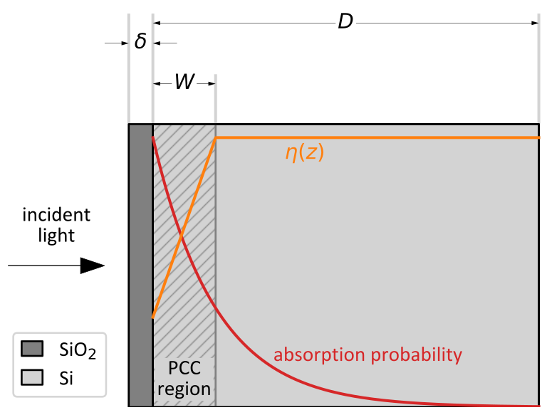
Photons are absorbed according to the Beer-Lambert law (red)
Photons absorbed in PCC region lose some electrons
Charge-collection efficiency (CCE) is the fraction of charge measured.
Piecewise-linear differential CCE introduced by Stern et al. (1994)
Denoted
Penetration depth
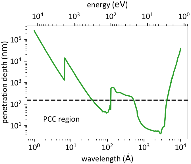
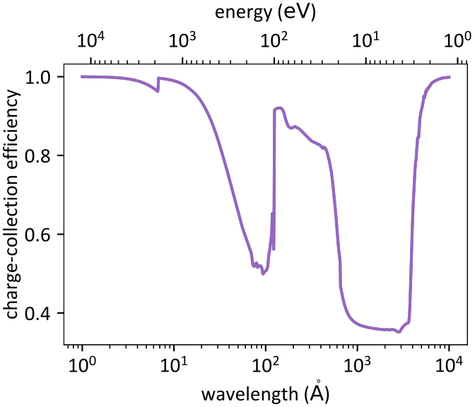
Some ultraviolet wavelengths have a penetration depth smaller than the PCC region
~40 – 100 A
~500 – 4500 A
Sensor is much less efficient in these regions
Average Charge-Collection Efficiency
Integrate Beer-Lambert law against differential CCE
Average CCE is needed for correct photometry
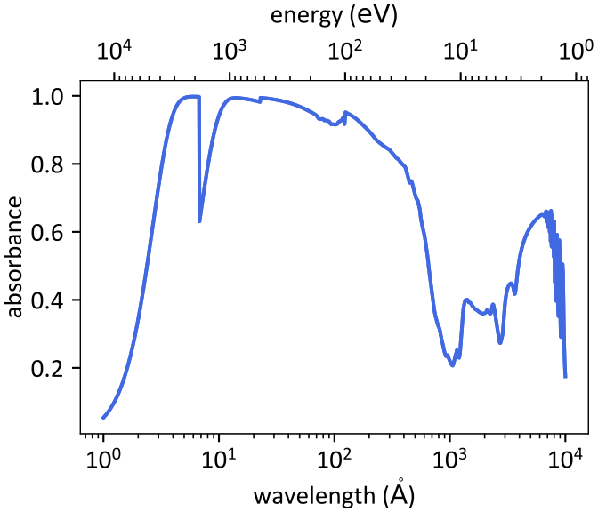
Absorbance
Energy absorbed by light-sensitive layer
Reflections from each interface
Oxide absorption
Transmittance through entire sensor
Computed using standard optical constants (Henke 1993, Palik 1997)
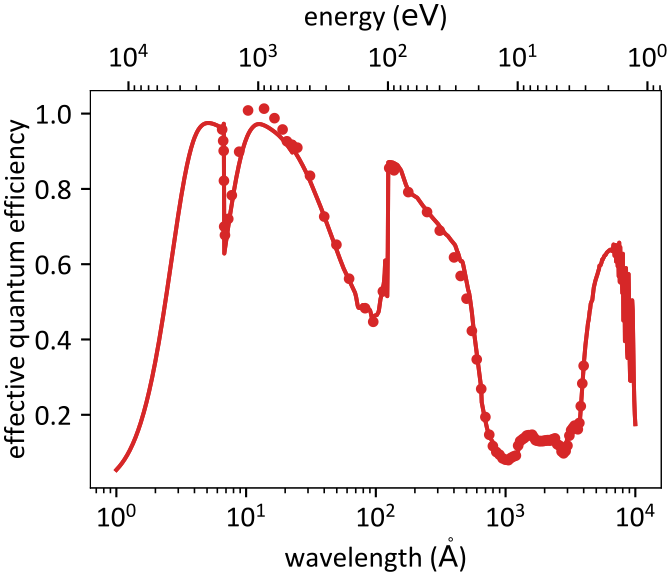
Effective Quantum Efficiency (EQE)
Measured quantity
Compare sensor to NIST photodiode
Between 0 and 1
Often used to compute QE
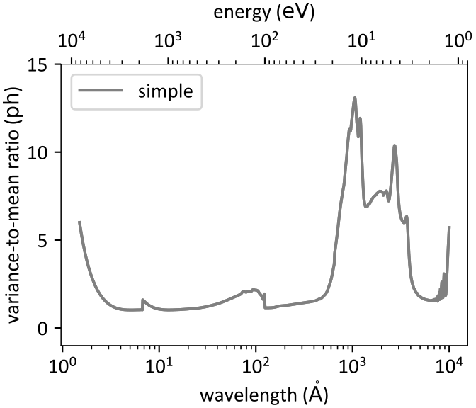
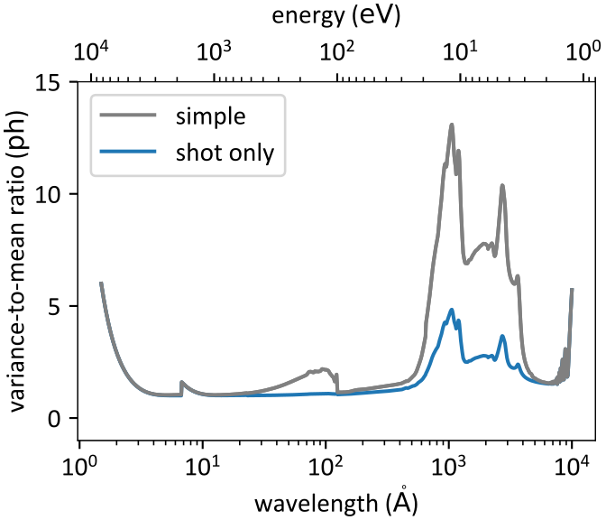
Simple Noise Model
Shot noise only
All-or-nothing charge collection
Used by IRIS and WFC3
Shot Noise
Absorbed photons are Poisson-distributed
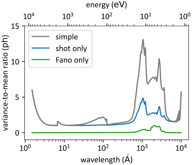
Fano Noise
Quantum yield uncertainty
Described by Fano factor
Ramanathan & Kurinksy (2020) QY model
Small compared to other noise sources
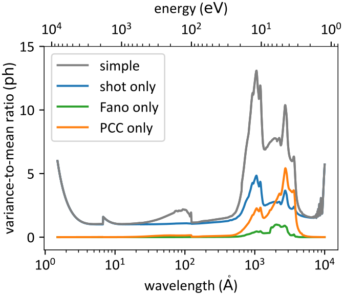
PCC Noise
Since each photon is absorbed at a different depth, each experiences a different CCE.
Total Noise
Sum of shot, Fano, and PCC noise
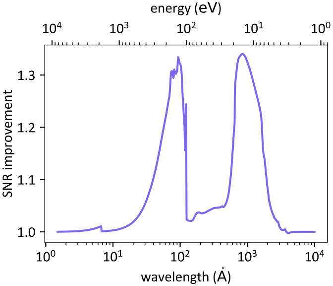
VMR is smaller than the simple model in the UV
The partial events improve the noise performance
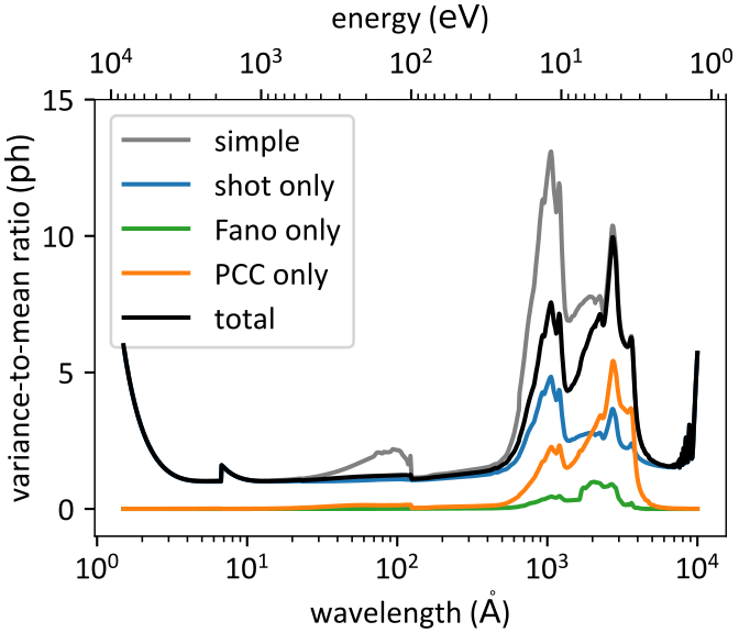
SNR improvement
SNR improves by up to compared to the simple model
Charge spreading?
Charge spreading is when electrons diffuse into adjacent pixels.
Proportional to size of field-free region
Could explain the discrepancy since this increases the correlations between pixels
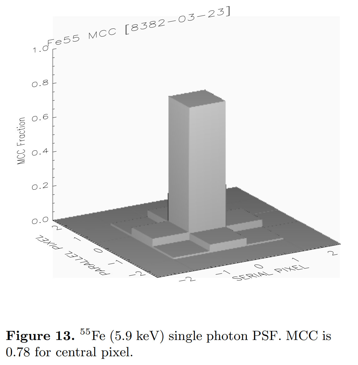
Stern et al. (2003)
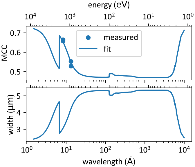
Mean Charge Capture (MCC)
Average fraction of charge captured by central pixel
Janesick (2001) charge spreading model
Stern et al. (2004) measurements
Fit size of field-free region
Predicts a similar amount of charge spreading for both UV and visible light
Compare to Measurements
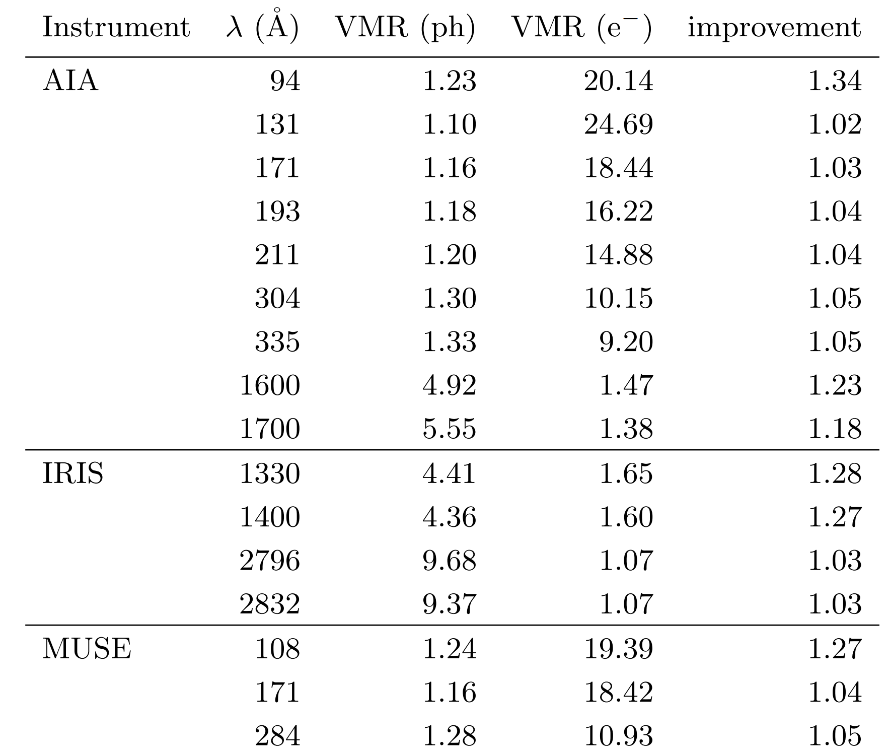
Affected Instruments
AIA
94 Å
1600 Å
1700 Å
IRIS
1330 Å
1400 Å
MUSE
108 Å